
The block diagram of Microprocessor 8085 is not a representation of the physical components, it is a gateway to comprehending how this microprocessor integrates and coordinates various units such as ALU, registers, and control units to execute instructions efficiently.
A microprocessor is an integrated circuit that understands and executes computer instructions. As well as performs various arithmetic and logical operations.
It is a multifunctional, clock-driven, register-based digital integrated circuit that receives binary data as input, processes it using instructions stored in its memory, and outputs results (also in binary form
Intel 4004 was the first commercially available microprocessor.
Continuous advancements in microprocessor capacity have rendered previous types of computers nearly outdated (see history of computing hardware), with one or more microprocessors included in everything from the tiniest embedded systems and portable devices to the giant mainframe computers and supercomputers.
Table of Contents
What is an 8085 Microprocessor?
8085 Microprocessor is 40 pin IC. It operates on a 3MHz frequency and +5V power supply.
Do you ever wonder why microprocessor 8085 is considered an 8-bit processor? No, I tell you. Because, at a time, it can fetch or execute only 8-bit data.
Also Read: What is Addressing Modes in 8085 Microprocessor?
Functional Block Diagram of Microprocessor 8085 | Pin Diagram of 8085 Microprocessor
This section of the blog post will give you a deep understanding of the FunctionalBlock Diagram of 8085 Microprocessor,
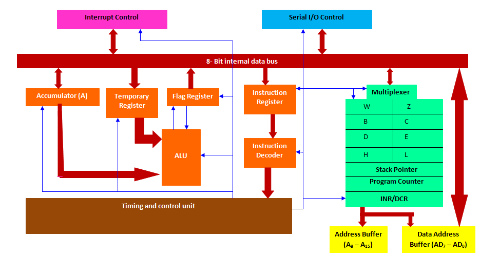
Address Bus and Data Bus
In 8085, the address bus is 16-bit (numbered A0-A15). This bus is linear, which means that bits move in only one way from the CPU unit to the peripheral devices, and it employs the high-order address bus. At the same time, the data bus is 8-bit.
AD0 – AD7 lines are multiplexed, which means these lines work as an address bus and a data bus. Bits A0– A7 carry lower order addresses, and bits A8 – A15 carry higher order addresses.
The question must have come to your mind: when will the AD0 to AD7 bit act as an address bus and when as a data bus? This thing is decided by Address Latch Enable (ALE). Let’s Understand What it is ALE?
Registers in Microprocessor 8085
The 8085 includes six general-purpose registers (B, C, D, E, H, and L) for storing 8-bit data. To execute some 16-bit operations, these can be joined as register pairs – BC, DE, and HL. These registers store or copy temporary data during program execution by utilizing instructions.
Accumulator
The accumulator is a component of the arithmetic and logical unit that is an 8-bit register (can hold 8-bit data) (ALU). The outcome of arithmetic or logical operations is kept in the accumulator. The accumulator can also be referred to as register A.
Flag Registers
The flag register is a special-purpose register that is distinct from the other registers of a microprocessor. It is an 8-bit register, in which only 5 are usable. The remaining three are empty and will be utilized in future Intel versions.
After an operation, these 5 flags are set or reset (when the value of the flag is 1, it is said to be set, and when the value is 0, it is said to be reset) based on the data condition of the result in the accumulator and other registers. The five flag registries are, Sign Flag, Zero Flag, Auxiliary Carry Flag (AC), Carry Flag,
Memory Registers
Memory addresses are stored in two 8-bit registers. Because memory addresses are 16 bits long, these registers are 16 bits long. They are as follows.
Program Counter (PC)
This is used to execute the instructions. The program counter’s role is to point to the memory address from which the next byte will be retrieved. When a machine code byte is retrieved, the program counter is increased by one to refer to the following memory address.
Stack Pointer
This type of pointer is utilized as a memory pointer. It refers to the stack, a region in read/write memory. During push and pop operations, it is always incremented/decremented by 2.
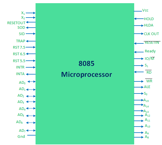
Status and Control Signals
Address Latch Enable (ALE)
This is a status and control signal. If its value is 1, AD0 to AD7 works as an address bus; otherwise, it acts as a data bus.
Input/Output or Memory (IO/M’)
A status signal indicates whether the data is fetched from input-output devices or memory. When it is set to high(1), the address on the address bus is for I/O devices. When it is set to zero, the address on the address bus is for memory.
S0 , S1 Signal
These are status indicators. They differ between several processes, such as stop, reading, instruction fetching, and writing.
| S0 | S1 | Read Operation |
| 0 | 0 | HALT |
| 0 | 1 | Read |
| 1 | 0 | Write |
| 1 | 1 | Opcode Fetch |
Read Signal (RD’)
This is a signal used to manage the READ operation. When it is low, the memory or input-output device of choice is read.
Write Signal (WR’)
It is a low-enabled signal. When it is low (0), it performs a WRITE operation. The data on the data bus is written into the specified memory or I/O destination.
Ready Signal
It detects whether or not a peripheral is ready to send data. If the value of READY is high(1), the peripheral is ready. If it is low(0), the CPU will wait until it is high. It’s handy for connecting low-speed devices.
Clock Frequency and Power Supply
Power supply Vcc – To operate, it needs a +5v power supply
Ground Reference – Vss
XI, X2 — These two pins are connected to a crystal oscillator. Because the frequency is internally split by two, a system operating at 3MHZ requires a crystal with a frequency of 6MHZ.
CLK (OUT) — Other devices can utilize this signal as the system clock.
Interrupts in Microprocessor 8085
The 8085 microprocessor supports five interrupt signals that can halt program execution for some time. INTR, RST 7.5, RST 6.5, RST 5.5
Signals for Reset
RESET IN’ — When this pin’s signal is low(0), the program counter is reset, the buses are tri-stated, and the microprocessor unit is reset.
Reset out: When this pin is set to 1 (high). All the external devices connected to the microprocessor will reset. Other devices can be reset when you press the reset button of the microprocessor.
DMA (Direct Memory Access) Signals
HOLD —When another device wants to utilize the address and data bus. Then, the DMA controller sends signal ‘1’ to the microprocessor, holds the current process, and frees the data bus and memory bus to access data from memory.
HLDA’ – It is a low enable signal that shows that a HOLD request has been received.
Serial I/O Ports
The two signals in 8085 implement serial communication.
SID and SOD
SID is a serial input data line, whereas SOD is a serial output data line. Whenever RIM Instruction is executed, data from this pin is loaded to the 7th bit of the accumulator. When SIM instruction is executed, the data is stored at the 7th bit of the accumulator and transferred to output devices.
Conclusion
The block diagram of 8085 microprocessor provides a simplified and comprehensive view of its internal structure, showcasing how various components interact to perform complex tasks.
This microprocessor is an 8-bit microprocessor and has components like an Arithmetic and Logic Unit (ALU), Registers, and Control Unit, Which work together to execute instructions, manage data, and communicate with external devices.
Its less power consumption and cost-effectiveness make it a practical choice for various applications.
But, this microprocessor has one limitation i.e. memory, Because of its limited memory, this microprocessor is unable to perform multitask and integrate with peripherals.
What aspect of the 8085 microprocessor’s block diagram do you find most intriguing, and how do you think it has influenced modern microprocessor design? Share your thoughts in the comments below.
Frequently Asked Questions (FAQs)
Q1: How many Pins are in the 8085 Microprocessor?
Ans: Microprocessor 8085 has 40 Pins.
Q2: What is PSW in a Microprocessor?
Ans: PSW means Program Status Word, which holds the status of arithmetic and logical operations of the CPU.
Q3: What is ALE Full Form in Microprocessor?
Ans: Full Form of ALE is Address Latch Enable.